Semiconductor Equipment
Semiconductor
Semiconductor
Process & Characterization
Equipment.
Moxie Lab supplies the complete semiconductor device fabrication workflow — from lithography and deposition through etching, metrology and photovoltaic instrumentation — for research centres and fabs across the UAE and GCC.
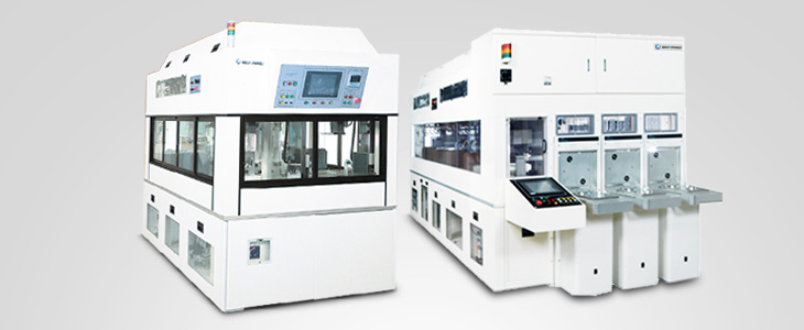
About Our Range
A complete portfolio of semiconductor process and characterization equipment covering diffusion, oxidation, lithography, deposition, etching, metrology, electrical testing and photovoltaic instrumentation — sourced from globally leading manufacturers.
Equipment Categories
settings_suggest
Diffusion, Oxidation & Deposition
- check_circleHorizontal & Vertical Diffusion Systems
- check_circleOxidation, Atmospheric & LPCVD Process Systems
- check_circlePECVD, ICP PECVD, ECR/Microwave Systems
- check_circleHV/UHV DC/RF Magnetron Sputtering Systems
- check_circleE-Beam & Thermal Evaporation
- check_circleUHV Deposition & MBE System for Oxides and Nitrides
- check_circleRapid Thermal Annealing System
grid_view
Lithography & Wet Process
- check_circlePhotolithography — Mask Aligner, UV Exposure Systems, Spin Coater, Developer, HMDS
- check_circleWet Process Stations — Spin Rinser Dryers, Spray Solvent Tool, Spray Acid Tool
- check_circleRIE, ICP-RIE System — Deep Silicon Etch
- check_circleLaser Pattern Generator

analytics
Metrology, Testing & Photovoltaics
- check_circleAutomated Defect Detection System
- check_circleNon Contact Optical Surface Profiler — BOW, WARP Metrology
- check_circleSpectroscopic Ellipsometer
- check_circleHall Effect Measurement System
- check_circleLED Tester & Probe Station — Manual, Semiautomatic, Fully Automatic
- check_circlePhotovoltaic Instrumentation — QE Measurement, Solar Simulator, I-V Tester, Solar Cell Sorter, Spectro Radiometer
Equip Your Semiconductor Lab.
Contact our team for full equipment lists, technical datasheets and pricing tailored to your fabrication needs.